Quick Answer: Silicon carbide (SiC) powder is the foundational material for modern semiconductors that power electric vehicles, solar energy systems, and high-performance electronics. Due to its wide bandgap, high thermal conductivity, and exceptional breakdown voltage, SiC powder is processed into single-crystal wafers used for SiC MOSFETs, Schottky diodes, and other next-generation power devices. These components outperform traditional silicon-based semiconductors in efficiency, temperature tolerance, and switching speed.
Table of Contents
- 1. Introduction
- 2. Why Silicon Carbide Is Revolutionizing the Semiconductor Industry
- 3. Physical and Electrical Properties of Silicon Carbide Powder
- 4. From SiC Powder to Semiconductor Wafers
- 5. Applications of SiC Semiconductors in Power Electronics
- 6. Advantages of SiC Over Silicon
- 7. Challenges and Future Outlook
- 8. FAQ
1. Introduction
The global shift toward energy efficiency and electrification has placed silicon carbide (SiC) at the center of semiconductor innovation. Unlike traditional silicon (Si), which has served the industry for more than five decades, SiC offers superior physical and electronic characteristics that meet the demands of modern power applications—particularly those requiring compact design, high voltage, and low energy loss.
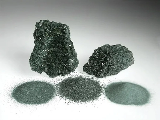
Silicon carbide powder is the raw form of this advanced material. Produced by reacting high-purity silicon dioxide (SiO₂) with carbon in electric furnaces, SiC powder serves as the foundation for wafers, substrates, and epitaxial layers used in power electronics. In its purest form, it enables the creation of wide-bandgap semiconductors that operate where traditional silicon devices fail—such as in electric vehicles, renewable energy systems, and aerospace technologies.
2. Why Silicon Carbide Is Revolutionizing the Semiconductor Industry
Semiconductors are the heart of modern electronics, controlling and converting energy efficiently. However, as power requirements rise and systems become more compact, traditional silicon-based components have reached their physical limits. Silicon can no longer handle the voltage, heat, or efficiency required by advanced systems without significant energy loss or large cooling systems.
Here, silicon carbide (SiC) enters the picture. SiC is known as a third-generation semiconductor material (after silicon and gallium arsenide). It has a bandgap of 3.26 eV—almost three times that of silicon (1.12 eV). This wider bandgap allows SiC-based devices to function under much higher voltages and temperatures while maintaining superior efficiency.
In addition to its electrical performance, SiC also provides excellent thermal conductivity (~490 W/m·K), mechanical strength, and chemical stability. These characteristics make it not only ideal for electronics but also for applications that operate in extreme conditions, such as space exploration and high-frequency telecommunications.
3. Physical and Electrical Properties of Silicon Carbide Powder
SiC powder’s effectiveness as a semiconductor material stems from its intrinsic crystal structure and atomic bonding. The strong covalent bond between silicon and carbon gives the compound hardness comparable to diamond and outstanding thermal and electrical performance.
| Property | Silicon Carbide (SiC) | Effect on Semiconductor Performance |
|---|---|---|
| Bandgap Energy | 3.26 eV (vs. 1.12 eV for Si) | Allows high-voltage operation and low leakage current |
| Thermal Conductivity | 490 W/m·K | Efficient heat dissipation, smaller cooling systems |
| Breakdown Electric Field | 3 MV/cm | Enables compact, high-power devices |
| Electron Mobility | 900 cm²/V·s | High switching speed, low power loss |
| Melting Point | ~2700°C | Stable under extreme fabrication and operating conditions |
These unique material traits make high-purity SiC powder essential for producing semiconductor-grade wafers capable of handling next-generation power demands.
4. From SiC Powder to Semiconductor Wafers
The journey from raw silicon carbide powder to a fully functional semiconductor device involves several sophisticated stages. Each step demands precision, purity, and advanced engineering.
4.1 Purification and Classification
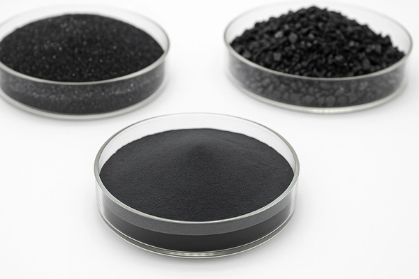
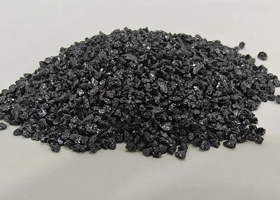
To meet semiconductor standards, SiC powder must have a purity level exceeding 99.9%. Trace metal impurities, oxygen, and free carbon are removed through chemical treatments and high-temperature refining. The powder is then classified into narrow particle size distributions to ensure uniform sintering and crystal growth.
4.2 Crystal Growth
Next, purified powder is used to grow single-crystal silicon carbide boules using methods such as the Physical Vapor Transport (PVT) or Chemical Vapor Deposition (CVD) technique. These processes are carried out at temperatures above 2500°C. The result is a large, defect-free crystal that serves as the base for slicing semiconductor wafers.
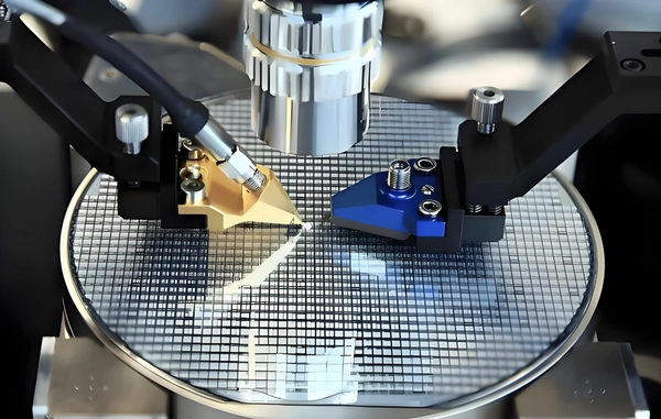
4.3 Wafer Slicing and Polishing
The SiC boule is precisely sliced into wafers using diamond or silicon carbide cutting abrasives. The wafers are then ground, lapped, and polished using fine powders of white fused alumina or brown fused alumina. Achieving mirror-smooth surfaces with minimal micro-defects is crucial to ensure stable electrical performance during chip fabrication.
4.4 Epitaxy and Device Fabrication
After polishing, an epitaxial SiC layer is grown on the wafer surface to fine-tune its electronic properties. Device structures such as SiC MOSFETs, Schottky diodes, and JFETs are fabricated through doping, etching, and metallization. These components are the building blocks for high-power electronic systems used in electric vehicles and renewable energy systems.
5. Applications of SiC Semiconductors in Power Electronics
The use of silicon carbide in semiconductors extends across multiple high-growth sectors where efficiency and durability are essential.
- Electric Vehicles (EVs): SiC MOSFETs used in main traction inverters reduce energy loss by up to 50%, increasing range and efficiency. Companies like Tesla and BYD already use SiC-based inverters in their vehicle platforms.
- Renewable Energy Systems: In solar inverters and wind power converters, SiC enables smaller designs, faster switching, and reduced thermal management requirements.
- Industrial Power Supplies: SiC power modules drive high-efficiency motor controls and robotics applications, operating reliably in harsh industrial conditions.
- Aerospace & Defense: SiC’s radiation hardness and high-temperature stability make it ideal for satellites, radar, and space power systems.
- 5G Base Stations: SiC-based RF amplifiers deliver higher power density and improved signal integrity in next-generation telecom infrastructure.
These applications demonstrate that SiC is not simply a replacement for silicon—it is the foundation of a new generation of power electronics.
6. Advantages of SiC Over Silicon
The comparison between SiC and Si highlights why the former is rapidly overtaking the latter in high-performance markets:
| Property | Silicon (Si) | Silicon Carbide (SiC) |
|---|---|---|
| Bandgap | 1.12 eV | 3.26 eV |
| Breakdown Voltage | ~300 V | >3000 V |
| Thermal Conductivity | 150 W/m·K | 490 W/m·K |
| Max Operating Temperature | 150°C | >600°C |
| Switching Efficiency | Moderate | Very High (Reduced losses) |
| Device Size | Larger, needs cooling | Compact, lightweight |
By using SiC powder–based components, manufacturers can create smaller devices that operate faster and more efficiently, reducing both cost and carbon footprint.
7. Challenges and Future Outlook
Despite its advantages, silicon carbide technology still faces challenges. The manufacturing process for SiC wafers is complex and energy-intensive, leading to higher costs compared to traditional silicon wafers. Crystal defects during growth, wafer fragility, and limited large-diameter availability (currently 6–8 inches) remain production hurdles.
However, the situation is changing rapidly. With global investments by leading semiconductor companies such as Wolfspeed, Infineon, Rohm, and STMicroelectronics, SiC wafer capacity is expanding dramatically. As the supply chain matures and economies of scale improve, the cost of SiC devices is expected to drop by 40–50% in the coming years.
For material suppliers, including CanAbrasive, high-purity SiC powder will continue to be a critical link between raw materials and the semiconductor industry. The development of consistent particle morphology, narrow size distribution, and minimal impurity levels will remain essential for meeting the growing demand for SiC-based power electronics.
8. FAQ
Why is silicon carbide powder essential in semiconductor manufacturing?
Because it serves as the fundamental raw material for SiC wafers. These wafers enable high-voltage, high-efficiency devices used in electric vehicles, solar systems, and industrial converters.
What purity level is required for semiconductor-grade SiC powder?
Semiconductor applications demand ultra-high-purity SiC powder with 99.9% or higher purity and minimal metallic or oxygen impurities.
Is SiC completely replacing silicon in the semiconductor industry?
No. SiC complements silicon by enabling applications that require higher performance, especially in power electronics and high-temperature environments where silicon is limited.
How does CanAbrasive support the semiconductor industry?
CanAbrasive supplies high-purity silicon carbide abrasives and powders for precision grinding, lapping, and wafer polishing, supporting both material production and semiconductor processing stages.